




404
+1-313-307-4176

Silicon Wafers Market | 2026-2034

Silicon Wafers Market Size, Share, Trend, Forecast, Competitive Landscape & Growth Opportunities: 2026-2034
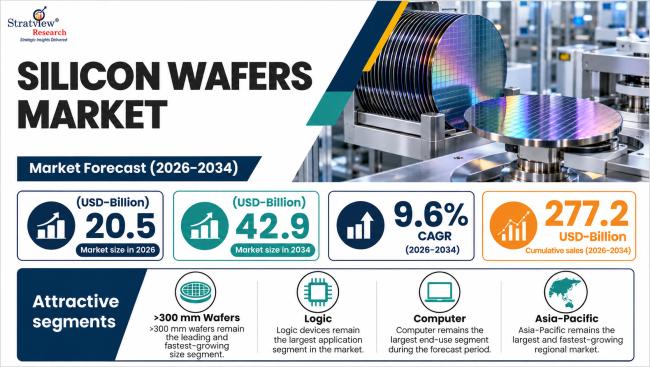
"The silicon wafers market is expected to reach USD 20.5 billion in 2026, growing 10.7% over 2025, and is projected to reach USD 42.9 billion by 2034, registering a CAGR of 9.6% during 2026–2034. The market is primarily driven by surging demand for AI processors and high-performance memory, which is increasing the need for high-quality 300 mm wafers. Expanding semiconductor fabrication capacity and regional investments in chip manufacturing are further supporting market growth."
The silicon wafers market was valued at USD 18.5 billion in 2025 and is expected to reach USD 20.5 billion in 2026, representing a year-on-year growth of 10.7%.
During the forecast period (2026–2034), the market is projected to grow at a CAGR of 9.6%, reaching USD 42.9 billion by 2034.
Asia-Pacific is projected to remain the leading regional market through 2026, supported by the region’s dense concentration of wafer fabrication capacity across Taiwan, Japan, South Korea, and China.
North America is expected to register the fastest growth during the forecast period.
>300mm wafers are expected to remain the leading and fastest-growing wafer size segment.
Logic devices are expected to remain the leading application segment in the years to come.
The computer segment is expected to remain the leading end-use industry, while communications is projected to register the fastest growth.
"As per the Senior Analyst at Stratview Research, the silicon wafers market is expected to create a cumulative sales opportunity of USD 277.2 billion during 2026-2034. During the upcoming years, >300mm Wafers, Logic Applications, Communication systems, and Asia-Pacific are some of the high-opportunity segments to bank upon."
Sharpen Your Strategies to Explore this USD 275 Billion+ Opportunity. Get a Free Sample of Our Report: "Here"
Have a look at the sales opportunities presented by the silicon wafers market in terms of growth and market forecast.
|
Market Statistics |
Value (in USD Billion) |
Market Growth (%) |
|
Market Size in 2025 |
USD 18.5 billion |
- |
|
Market Size in 2026 |
USD 20.5 billion |
YoY Growth in 2026: 10.7% |
|
Market Size in 2034 |
USD 42.9 billion |
CAGR 2026-2034: 9.6% |
|
Cumulative Sales Opportunity during 2026-2034 |
USD 277.2 billion |
- |
Want to Explore the Market Opportunities? Get a Free Sample "Here"
The silicon wafers market is gaining momentum from rising demand for AI chips and data center infrastructure, increasing semiconductor fabrication capacity, and growing investment in advanced chip manufacturing. The shift toward advanced semiconductor processes and high-performance computing is strengthening the need for high-quality silicon wafers, particularly 300 mm wafers used in large-scale chip production. Meanwhile, government-backed semiconductor manufacturing initiatives in the United States and capacity expansion across Asia are influencing regional production and supply chains. However, high capital investment requirements, fluctuations in semiconductor demand and wafer pricing, and the technical challenges of maintaining stringent wafer quality standards continue to pose challenges for market participants.
Growing Demand for AI Chips and Data Center Infrastructure
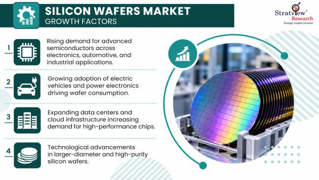
The growing demand for artificial intelligence (AI) chips and data center infrastructure is driving the silicon wafers market. AI servers require advanced logic processors, high-bandwidth memory (HBM), dynamic random-access memory (DRAM), and storage chips, all of which rely on silicon wafers during semiconductor manufacturing. According to the Semiconductor Industry Association (SIA), annual revenue from semiconductors deployed in AI data centers could exceed USD 1.2 trillion by 2028. As cloud providers expand AI computing and storage infrastructure, demand for the advanced logic and memory chips powering these systems increases, supporting consumption of the silicon wafers used to manufacture them.
Increasing Semiconductor Content in Automotive and Industrial Applications
The growing use of electronics in automotive and industrial applications is broadening demand for silicon wafers beyond data center-related technologies. Vehicles use semiconductors for power management, electronic control, safety systems, and advanced driver-assistance systems, while industrial equipment relies on chips for automation, sensing, and motion control. Gartner forecasts that automotive semiconductor content per vehicle will increase from USD 860 in 2024 to USD 1,902 in 2034, driven by vehicle electrification and autonomous-driving technologies. As vehicles incorporate more electronic functions, the value and complexity of their semiconductor systems increase, supporting demand for silicon wafers used in automotive chip production. Industrial automation provides an additional source of demand across manufacturing and equipment applications.
Expansion of Advanced Semiconductor Manufacturing Capacity
Investment in semiconductor fabrication capacity supports the silicon wafers market by enabling chipmakers to manufacture greater volumes of semiconductor products. SEMI forecasts that global spending on 300 mm semiconductor fabrication equipment will reach USD 133 billion in 2026 and USD 151 billion in 2027. This investment supports the installation and upgrading of production equipment across semiconductor fabrication facilities. As new production lines become operational and existing facilities increase output, their requirements for silicon wafers can rise. However, the impact on wafer demand depends on the pace of capacity ramp-up, factory utilization, and the types of chips being manufactured.
"As per our analyst, the silicon wafers market is driven by rising demand for AI processors and high-performance memory, which is increasing the need for high-quality 300 mm wafers. Expanding semiconductor fabrication capacity and regional investments in chip manufacturing are further supporting market growth."
Align with the Mega Trends Shaping the Industry. Get a Free Sample "Here"
Semiconductor Market Volatility and Pricing Pressure
The silicon wafers market is vulnerable to fluctuations in semiconductor demand, inventory corrections, and changes in wafer pricing. Demand can vary across end-use industries, with advanced computing applications experiencing different market conditions from automotive, industrial, and consumer electronics. These fluctuations make it difficult for silicon wafer manufacturers to align production volumes with customer demand, manage inventory, and maintain profitability during market downturns. Even when shipment volumes recover, pricing pressure can limit revenue growth.
High Manufacturing Complexity and Quality Requirements
Silicon wafer manufacturing requires precise control over crystal growth, material purity, wafer thickness, surface flatness, and defect levels. As semiconductor fabrication processes become more demanding, wafer manufacturers must maintain increasingly stringent specifications to ensure consistent chip performance and production yields. Meeting these requirements calls for specialized equipment, advanced process controls, and rigorous quality assurance, increasing manufacturing complexity and the technical barriers to entry.
"Wafers larger than 300 mm are expected to remain the dominant segment over the years to come."
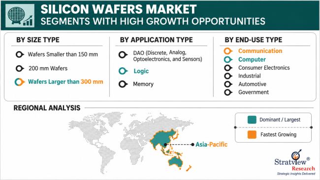
Based on size type, the silicon wafers market is segmented into wafers smaller than 150 mm, 200 mm wafers, and wafers larger than 300 mm. Wafers larger than 300 mm are expected to maintain their leading position as semiconductor manufacturers seek to produce more chips from each wafer, improving manufacturing productivity and cost efficiency. Their use in advanced logic and memory fabrication supports demand from high-performance computing, AI processors, and data center applications. As chipmakers expand production of these technologies, demand for larger-diameter silicon wafers is expected to remain strong.
"Logic devices are projected to remain the largest application segment in the silicon wafers market."
Based on application type, the market is segmented into DAO (discrete, analog, optoelectronics, and sensors), logic, and memory. Logic devices are expected to remain the largest segment because they perform the processing and control functions required in computing systems, smartphones, networking equipment, and AI accelerators. Increasing computational workloads and demand for high-performance processors support production of advanced logic chips, which in turn drives demand for the silicon wafers used in their fabrication. Memory wafers also benefit from growing data storage requirements and AI-related demand, while DAO wafers serve power management, sensing, and signal-conversion applications.
Get Insights on High-Growth Segments. Get a Free Sample "Here"
"Computer is expected to remain the largest end-use segment during the forecast period."
Based on end-use type, the silicon wafers market is segmented into communication, computer, consumer electronics, industrial, automotive, and government. Computer is expected to remain the largest end-use segment, supported by demand for processors, memory, and other semiconductor components used in personal computers, servers, and data center systems. The expansion of cloud computing and AI workloads increases the need for computing infrastructure, prompting semiconductor manufacturers to produce more advanced logic and memory chips. This supports demand for silicon wafers used in computer-related semiconductor applications. Communication and automotive applications provide additional demand through networking equipment and vehicle electronics.
"Asia-Pacific is expected to remain the largest and fastest-growing regional market over the upcoming years."
Asia-Pacific is expected to maintain its leading position in the silicon wafers market because of its extensive semiconductor manufacturing ecosystem, concentration of chip fabrication facilities, and strong presence in electronics production. Countries such as China, Taiwan, South Korea, and Japan play important roles in semiconductor manufacturing and related supply chains. Continued investment in fabrication capacity and demand for chips used in computing, memory, communication, and consumer electronics support regional silicon wafer consumption. As semiconductor manufacturing capabilities expand across the region, Asia-Pacific is also expected to register the fastest growth during the forecast period.
Speak to Us for Deep-Diving into a Country/Region-Specific Opportunity. Contact Us "Here"
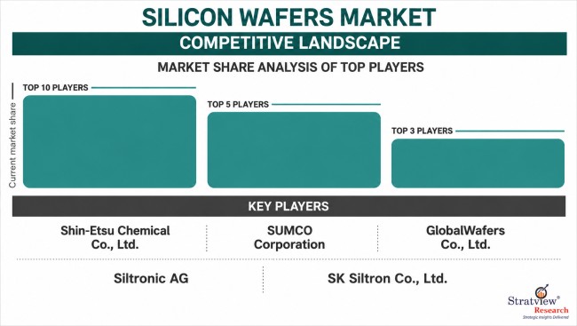
The silicon wafers market features the presence of several well-established semiconductor materials companies offering monocrystalline, polycrystalline, and epitaxial wafers across 150mm, 200mm, and 300mm diameters to logic, memory, analog, and power semiconductor manufacturers. Most major players compete on wafer purity, defect density, diameter capability, and long-standing supply relationships with leading chipmakers and foundries.
The following are the key players in the silicon wafers market.
Shin-Etsu Chemical Co., Ltd.
SUMCO Corporation
GlobalWafers Co., Ltd.
Siltronic AG
SK Siltron Co., Ltd.
Note: The above list is not an exhaustive list of the key players in the market. If your company is active in this market and would like to be considered for inclusion in future editions of this study, please contact us at [email protected].
Have the Competitive Edge with Our Intelligence. Get a Free Sample "Here"
In July 2026, GlobalWafers Co., Ltd. announced a strategic collaboration with Micron Technology to strengthen the U.S. semiconductor supply chain. The proposed arrangement includes USD 500 million in strategic financing support from Micron for GlobalWafers’ U.S. manufacturing operations and plans for a 10-year long-term supply agreement. The collaboration is intended to strengthen the supply of advanced silicon wafers for memory manufacturing and support demand driven by artificial intelligence and data centers.
In June 2026, Siltronic AG completed a capital increase that generated EUR 273 million in gross proceeds through a private placement of new shares. The company intends to use the proceeds to strengthen its balance sheet, support its growth strategy, and maintain investment flexibility for its advanced silicon wafer business.
In September 2025, Siltronic AG announced a collaboration with cosine to supply high-quality 300 mm silicon wafers for silicon-pore optics used in the European Space Agency’s NewAthena X-ray telescope. The partnership demonstrates the application of high-uniformity silicon wafer technology in specialized optical systems beyond conventional semiconductor manufacturing.
In May 2025, GlobalWafers Co., Ltd. officially opened its GlobalWafers America facility in Sherman, Texas, for 300 mm silicon wafer manufacturing. The company also announced plans to increase its intended U.S. investment from USD 3.5 billion to USD 7.5 billion, including proposed additional expansion phases. The development is aimed at strengthening domestic wafer manufacturing capabilities and the resilience of the U.S. semiconductor supply chain.
The silicon wafers market encompasses thin, high-purity discs of silicon sliced from monocrystalline or polycrystalline ingots that serve as the foundational substrate for semiconductor device fabrication. Produced primarily through the Czochralski crystal-growth process and subsequently sliced, lapped, polished, and in some cases epitaxially coated, silicon wafers are available across a range of diameters, including 150mm, 200mm, and 300mm. These wafers form the base material on which integrated circuits, memory chips, logic processors, analog devices, and power semiconductors are fabricated, supporting applications across communication, computing, consumer electronics, automotive, and industrial end markets.
This report provides the most comprehensive market intelligence. The report structure has been kept so that it offers maximum business value. It provides critical insights into market dynamics and will enable strategic decision-making for existing market players and those looking to enter the market.
The following are the key features of the report:
Market structure: Overview, industry life cycle analysis, supply chain analysis.
Market environment analysis: Growth drivers and constraints, Porter’s five forces analysis, SWOT analysis.
Market trend and forecast analysis.
Market segment trend and forecast.
Competitive landscape and dynamics: Market share, product portfolio, new product launches, etc.
Attractive market segments and associated growth opportunities.
Emerging trends.
Strategic growth opportunities for the existing and new players.
Key success factors.
|
Market Study Period |
2020-2034 |
|
Base Year |
2025 |
|
Forecast Period |
2026-2034 |
|
Trend Period |
2020-2025 |
|
Number of Tables & Figures |
100+ |
|
Number of Segments Analysed |
5 (Wafer Size, Type, Application, End-Use Industry, and Region) |
|
Number of Regions Analysed |
4 (North America, Europe, Asia-Pacific, Rest of the World) |
|
Countries Analysed |
16 (The USA, Canada, Mexico, Germany, France, The UK, Italy, China, Japan, South Korea, Taiwan, India, Singapore, Rest of Europe, Rest of APAC, and Rest of the World) |
|
Free Customization Offered |
10% |
|
After Sales Support |
Unlimited |
|
Report Presentation |
Complimentary |
|
Market Dataset |
Complimentary |
|
Further Deep Dive & Consulting Services |
10% Discount |
Want a Report Tailor-Made to Your Objectives? Speak with Our Analyst.
The report provides detailed insights into market dynamics to enable informed business decision-making and the formulation of growth strategies based on market opportunities.
The silicon wafers market is segmented into the following categories:
Silicon Wafers Market, By Wafer Size
150mm
200mm
300mm
Others
Silicon Wafers Market, By Type
Monocrystalline
Polycrystalline
Others
Silicon Wafers Market, By Application
Memory
Logic/MPU
Analog & Discrete
Others
Silicon Wafers Market, By End-Use Industry
Communication
Computer
Consumer Electronics
Industrial
Automotive
Others
Silicon Wafers Market, By Region
North America (Country Analysis: The USA, Canada, and Mexico)
Europe (Country Analysis: Germany, France, The UK, Italy, and Rest of Europe)
Asia-Pacific (Country Analysis: China, Japan, South Korea, Taiwan, India, and Rest of Asia-Pacific)
Rest of the World (Country Analysis: Singapore and Others)
Looking for a Deep Dive? Speak with Our Analyst.
This strategic assessment report from Stratview Research provides a comprehensive analysis that reflects today’s silicon wafers market realities and future market possibilities for the forecast period.
The report segments and analyzes the market in the most detailed manner to provide a panoramic view of the market. The vital data/information provided in the report can play a crucial role for market participants and investors in identifying the low-hanging fruits available in the market and formulating growth strategies to expedite their growth process.
This report offers high-quality insights and is the outcome of a detailed research methodology comprising extensive secondary research, rigorous primary interviews with industry stakeholders, and validation and triangulation with Stratview Research’s internal database and statistical tools.
More than 1,000 authenticated secondary sources, such as company annual reports, fact books, press releases, journals, investor presentations, white papers, patents, and articles, have been leveraged to gather the data.
We conducted more than 15 detailed primary interviews with market players across the value chain in all four regions and industry experts to obtain both qualitative and quantitative insights.
With this detailed report, Stratview Research offers one of the following free customization options to our respected clients:
Company Profiling
Detailed profiling of additional market players (up to three players).
SWOT analysis of key players (up to three players).
Competitive Benchmarking
Benchmarking of key players on the following parameters: product portfolio, geographical reach, regional presence, and strategic alliances.
Custom Research: Stratview Research offers custom research services across industries. In case of any custom research requirement related to market assessment, competitive benchmarking, sourcing and procurement, target screening, and others, please send your inquiry to [email protected].
The report is delivered digitally through our online portal. Buyers receive login credentials from our team to access the report and may update their credentials at any time after the initial login.
Delivery timelines depend on the status of the report:
For the most accurate delivery timeline, please contact us to confirm the current status of the report.
Yes. You may request a complimentary preview of the report through a video conference with our team.
Yes. The scope of the report can be fully customized to align with your specific research objectives and information requirements.
Please contact us at [email protected], and our team will be happy to discuss your requirements and propose a tailored solution.
Yes. Selected sections of the report can be purchased separately based on your requirements. Please contact us at [email protected] to discuss your needs.
Yes, AI can help gather publicly available information, but its outputs are only as reliable as the data it accesses. Stratview Research reports are built using validated data, extensive primary interviews with industry stakeholders, and the expertise of our experienced research team.
Additionally, many critical insights, including market dynamics, competitive intelligence, and industry-specific trends, are not publicly available and therefore cannot be captured through AI alone.
Silicon wafers market size was USD 18.5 billion in 2025. The market is expected to grow from USD 20.5 billion in 2026 to USD 42.9 billion in 2034, witnessing a robust market growth (CAGR) of 9.6% during the forecast period (2026-2034).
Shin-Etsu Chemical Co., Ltd., SUMCO Corporation, GlobalWafers Co., Ltd., Siltronic AG, and SK Siltron Co., Ltd. are the leading players in the silicon wafers market.
Asia-Pacific holds the largest share in the silicon wafers market, supported by its dense concentration of semiconductor foundries and wafer fabrication capacity across Taiwan, Japan, South Korea, and China, along with the presence of leading wafer manufacturers in the region.


WE ACCEPT