According to insights from Stratview Research, a steady shift toward these emerging trends is expected to open new revenue streams for market players, with the PCB laminates market projected to reach nearly US$ 20.5 billion by 2027.
Electronics Industry is one of the rapidly evolving industries that is driven by innovations. To keep up the pace, the players have to keep upgrading their products and services. One of the significant upgrades is the decreasing size of electronics.
Also, electronics have become more prevalent in consumer goods, and the pressure of miniaturizing the products has pushed the manufacturers to search for better solutions. Thus came PCBs – Printed Circuit Boards. To prevent any sort of conduction of signals or current, the PCBs have conductive pathways etched and laminated with multiple sheets.
Pcbs Have a Huge List of Applications
A few most common PCB applications by industry are –
- Consumer Electronics (like television, microwaves, refrigerators, etc.),
- Automotive industry (for digital displays, Sensors, Radar system, etc.),
- Aviation industry (radar installation, aerospace sensors, power supplies and converters, electronic flight instrumentation, etc.)
- Industrial Electronics (like power supplying equipment, etc.),
- Medical devices (including drug delivery systems, hearing aids, wearable devices, etc.).
- Computers and Peripherals - PCBs are an integral part of computing, storage, and peripherals. Growing use of computers, laptops, etc. is pushing the demand for PCBs in this sector.
- More than 335 million units of computers were sold in the year 2021. Applications in this particular segment accounted for ~23% of the PCB laminates market.
- Communications – High quality, light-weight PCB laminates are the lifeblood for any communicational device such as Smart phones, Computers, Radio, etc.
PCBs deliver different stability level and performance to all the above applications. The major role in this is played by the laminates that are used while manufacturing PCBs, as PCB laminates are what binds and holds the layers of components together.
Mobile Subscribers and 5g Enabled Phones to Boost Demand for PCBLaminates
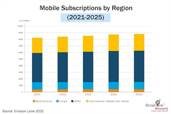
The soaring demand in communication industry due to the advancements and improvements in data transmission possibilities, etc. makes it the largest application of the PCBs and PCB laminates. According to Ericsson, one of the leading providers of Information and Communication Technology (ICT), the number of mobile subscriptions is projected to increase from 8.2 billion by the end of 2021 to more than 9 billion by 2027.
The global count of 5G subscribers is also growing rapidly. Estimates suggest that 5G will become the prevailing mobile access technology by subscriptions in the year 2027 with over 4.4 bn subscriptions globally, accounting for 48% of all mobile subscriptions.

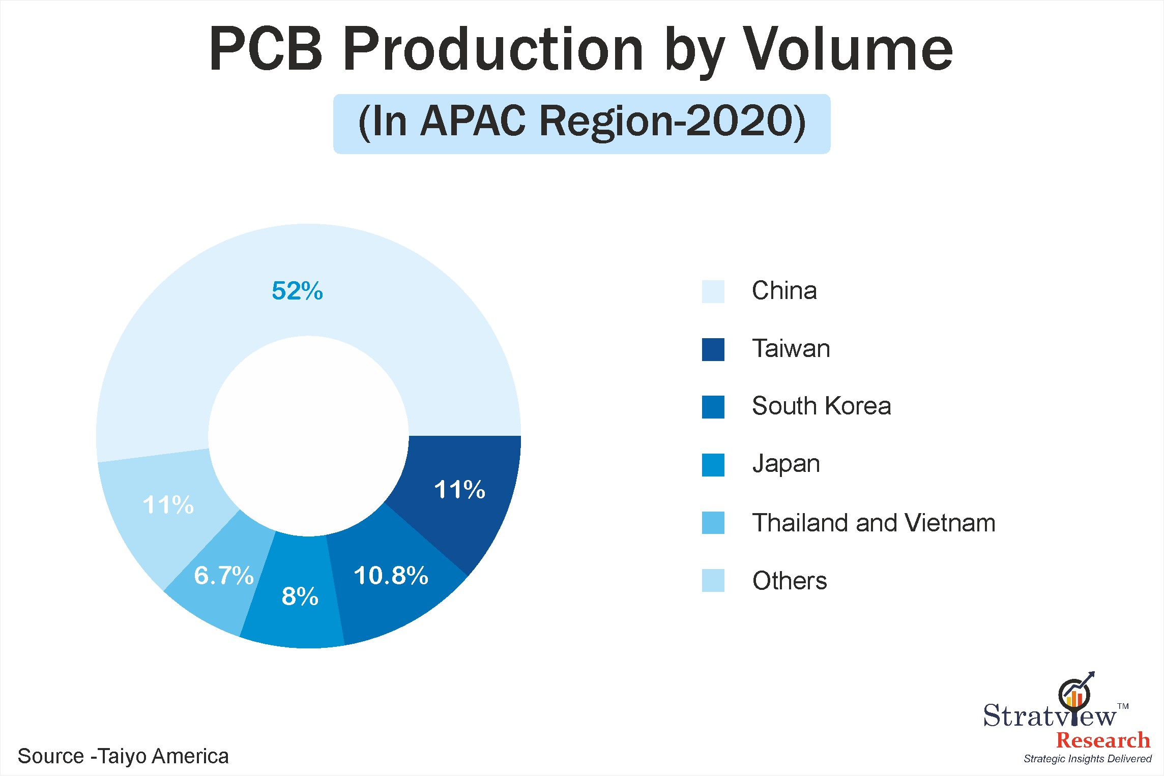
Fig 1: PCB Production by Volume (in Asia Pacific Region - 2020)
To meet such growing demand, mobile manufacturers have been focusing on accelerating production which parallelly increases the demand for PCB laminates. Majority of mobile subscribers come from Asia-Pacific. Also Asia-Pacific accounted for >85% of PCB production in 2020, (Figure above depicts the share of production of PCBs in APAC region), this region boasts the largest PCB production base across the globe.

Fig. 2 : Mobile Subscriptions By Region
Do All Industries Use the Same Type of PCBs?
No. You’ll find the terms ‘single-sided’, ‘double-sided’, and ‘multilayer’ or ‘Rigid’, ‘flexible PCBs’, and ‘HDI PCB’ (stands for High-Density Interconnect), often when you read information about PCBs. The PCB manufacturers use these terms to categorize the complexity of a board’s structure.
Single-Sided PCBs– Ideal for simple low-density designs, these boards are used usually in Radios, Coffee Makers, Camera Systems, etc.
Double-Sided PCBs– There are limitless applications of double-sided PCBs. Examples include - Industrial Controls, UPS systems, Regulators, etc.
Multilayer PCBs – Having higher assembly density, and increased flexibility, these multilayer PCBs are used more than any other type. Examples of applications of Multilayer PCBs are – Computers, Mobile devices, medical devices such as Heart monitors, X-ray Equipment, etc.
Rigid PCBs - A rigid PCB board is made of ceramic or glass. Durable enough to withstand high heat and prolonged exposure to the elements, this is used in devices like printers, etc.
Flexible PCBs – A flexible printed circuit is a form of conductors printed onto a flexible insulating film - can also be used in military and space application
PCB manufacturers have seen an increased demand for rigid-multilayer boards, a combination of multilayer and rigid PCBs, due to the need for smaller, and complex devices. These combination Multilayer-Rigid boards by their innate versatile properties provide multiple benefits such as –
- High capacity and high speed in a smaller footprint,
- Reduced or almost no need for connectors required for multiple layers of PCBs,
- Simplified construction, and
- Reduced weight.
What are These PCBs Made of?
These flat laminated composites can be made of either one/two layers of copper, or in high density applications, these can have as much as 40 or 50 layers or even more. While manufacturing PCB, the manufacturers look for the following characteristics in the laminates used in PCBs–
- Dielectric constant,
- Fire retardance,
- Tensile strength,
- Glass transition temperature,
- Shear strength, and more.
What is the commonly used laminate type? How, and why does it stand ahead of others?
|
Laminates |
Characteristics |
Materials used |
|
FR – 4 |
Flame-resistant material, good thermal, electrical, and mechanical characteristics, a favourable strength-to-weight ratio makes it ideal for most devices. |
Woven fiberglass cloth with an epoxy resin binder. |
|
High Tg (glass transition temperature) |
Superior thermal performance, and chemical resistance. Offers excellent electrical insulation in devices with extreme humidity and temperatures. |
Copper-coated laminate treated by internal layer imaging along with PREPREG layers application. |
|
CEM (Composite Epoxy Material) |
Comes in 5 variants. CEM-1 is low-cost, cellulose-paper-based laminate with only one layer of woven glass fabric. CEM-2 has cellulose paper core & woven glass fabric surfaces. CEM-3 (similar to FR-4) is white in colour and is flame-retardant. CEM-4 (similar to CEM-3) is not flame-retardant. CEM-5 (also called CRM-5) has polyester woven glass core. |
Layers of woven glass fabric and paper (cellulose) along with epoxy (source -pcbdirectory) |
|
Halogen Free FR-4 |
Phosphorus or nitrogen materials are used to replace halogens as frame-retardants, they have smaller thermal expansion coefficient, and moisture-absorption rate. |
Halogen-free copper-clad (phosphorus and phosphorus-nitrogen) |
Table 1. Some of the Types of Laminates and Their Characteristics
Fr-4 - the Widely Used Material for PCBs
The favourable characteristics and properties of ‘FR4’ support its widespread usage. FR4 laminates are made from fiberglass cloth, epoxy resin, and are usually the lowest cost laminates available for PCBs.
Below given are a few characteristics of FR4 PCB Laminates–
- Flame retardance – FR4 laminates are flame-retardant systems of woven glass covered with epoxy-like resin. These laminates gain their fire-retardancy from the presence of the halogen chemical element bromine.
- Good electrical properties – The electric properties of FR4 PCB laminates are critical for signal integrity. They specify how fast an electrical signal propagates through the material and how much electric charge it can retain.
- Low moisture absorption – This property makes FR4 PCB laminate material highly resistant to water and delamination. FR4 materials offer a low moisture absorption of 0.1% even when immersed in water for 24 hours.
- Cost effectiveness- These materials are cost friendly when compared to other materials.
What Are the Trends Powering the Pcb Market?
Efforts to eliminate substances deemed environmentally unfriendly are already impacting the PCB laminates market. This trend opens the doors for ‘halogen-free’ laminates. The use of halogen as a flame-retardant, which emits a large amount of highly toxic gas, is being replaced by phosphorus and phosphorus-nitrogen.
These ‘halogen-free’ laminates provide good stability, improved insulation, and water absorption properties, due to which they are more expensive, compared to conventional PCBs.
The shift toward miniaturization is giving rise to the increased High-Density Interconnect (HDI) techniques. HDI allows fewer layers on board yet provides amazing signal transmission speed.
‘Tech-friendly’ PCB laminates can be the next big thing in the PCB market. ‘Internet of Things’ is something, that is widely being applied in manufacturing smart home/work appliances, smart wearable devices, and automotive LCD displays, etc. According to latest statistics on IoT devices, the number of devices connected to IoT will exceed 3.5 billion by 2023. And by 2025, there will be >152,000 IoT devices connecting to the internet every minute.
PCB Laminates have been transforming over the years. After the hit of COVID-19, a deficit in ‘copper’ supplies, the prime element needed for manufacturing PCBs, lead to the increase in prices of raw materials. Although, due to the high demand for electronic devices, the market is slowly and steadily growing.
A gradual shift towards such trends is likely to create new revenue pockets for the market players and by 2027, the PCB laminates market may touch US$ 20.5 Billion value.
Changing Landscapes
There are a few instances that can possibly change the present prospect of the PCB laminates Market. Such as govt schemes like ‘Production Linked Incentive Scheme’ (PLIs, by Indian Govt.) are encouraging tech giants to shift their production units to India. Similarly, rising geopolitical tensions, like US-China trade war, supply chain crunches amid the pandemic, etc. are forcing several giants like Google, Apple, etc. to move their units to nearby countries.
For instance –
- Apple has diversified its supply chains from China and started manufacturing iPhone 14 in India and iPads & watches in Vietnam as tensions rise between Washington and Beijing.
- Rising labour costs in South Korea, and China has pushed Samsung to discontinue its mobile production in these regions and shift to countries like India, and Vietnam.
Irrespective of the other developments in the industry, the changing manufacturing landscape for electronics is worth noticing. With the growing consumer demands for smarter, and miniaturized products, industries now are focus on accelerating their productions.
The future of the PCB industry, thus, is luminous, shaped by product performance and miniaturization to make the lives easier.
Authored by Stratview Research. Also published on – EE Power
